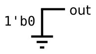
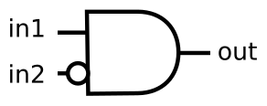
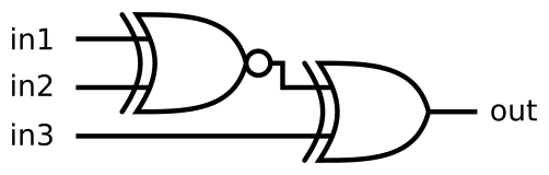
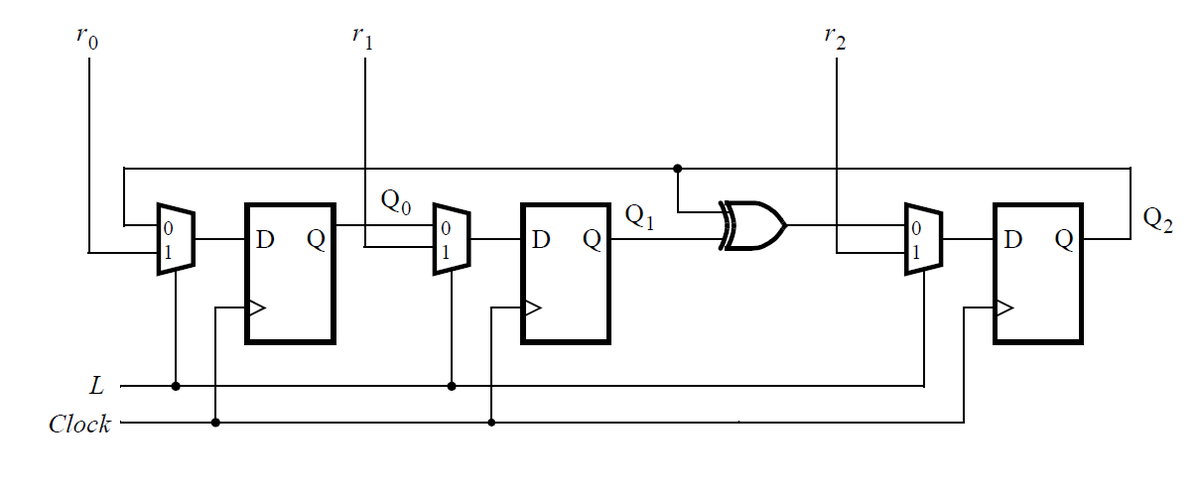
习题:We’re going to start with a small bit of HDL to get familiar with the interface used by HDLBits. Here’s the description of the circuit you need to build for this exercise:
Build a circuit with no inputs and one output. That output should always drive 1 (or logic high).
搭建一个没有输入,只有一个输出的电路。且输出始终为1即高电平。
verilog
module top_module (output one); assign one = 1'b1;endmodule
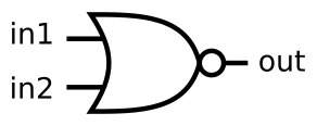
习题:Create a module that implements a NOR gate. A NOR gate is an OR gate with its output inverted. A NOR function needs two operators when written in Verilog.
搭建一个具有或非门功能的模块。或非门是对一个或门的输出取反。或非门用Verilog描述时需要两步。
verilog
module top_module( input a, input b, output out); assign out = ~(a | b);endmodule
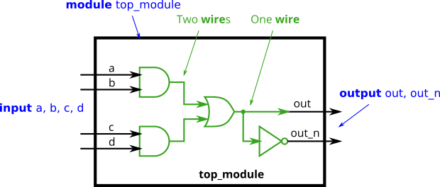
习题:Implement the following circuit. Create two intermediate wires (named anything you want) to connect the AND and OR gates together. Note that the wire that feeds the NOT gate is really wire out, so you do not necessarily need to declare a third wire here. Notice how wires are driven by exactly one source (output of a gate), but can feed multiple inputs.
If you’re following the circuit structure in the diagram, you should end up with four assign statements, as there are four signals that need a value assigned.
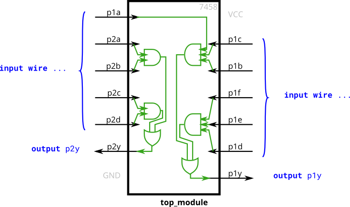
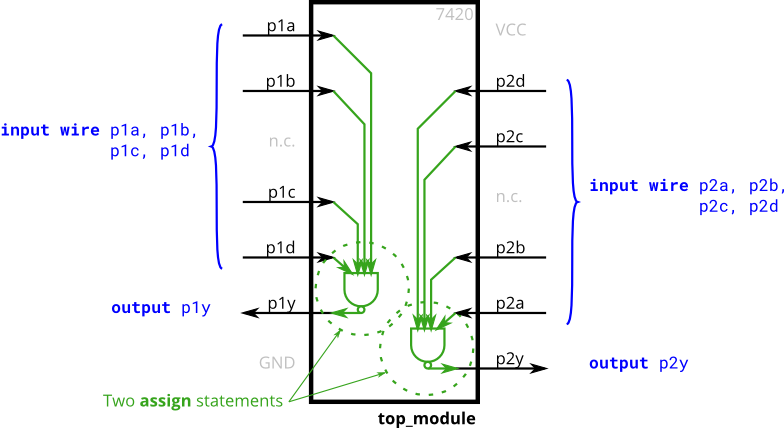
习题:Create a module with the same functionality as the 7458 chip. It has 10 inputs and 2 outputs. You may choose to use an assign statement to drive each of the output wires, or you may choose to declare (four) wires for use as intermediate signals, where each internal wire is driven by the output of one of the AND gates. For extra practice, try it both ways.
习题:Build a circuit that has one 3-bit input, then outputs the same vector, and also splits it into three separate 1-bit outputs. Connect output o0 to the input vector’s position 0, o1 to position 1, etc.
习题:A 32-bit vector can be viewed as containing 4 bytes (bits [31:24], [23:16], etc.). Build a circuit that will reverse the byte ordering of the 4-byte word.
习题:Build a circuit that has two 3-bit inputs that computes the bitwise-OR of the two vectors, the logical-OR of the two vectors, and the inverse (NOT) of both vectors. Place the inverse of b in the upper half of out_not(i.e., bits [5:3]), and the inverse of a in the lower half.
习题:Given several input vectors, concatenate them together then split them up into several output vectors. There are six 5-bit input vectors: a, b, c, d, e, and f, for a total of 30 bits of input. There are four 8-bit output vectors: w, x, y, and z, for 32 bits of output. The output should be a concatenation of the input vectors followed by two 1 bits。
习题:Build a circuit that sign-extends an 8-bit number to 32 bits. This requires a concatenation of 24 copies of the sign bit (i.e., replicate bit[7] 24 times) followed by the 8-bit number itself.
搭建一个电路用于将8位数字符号扩展到32位。这要求将8位数字的符号位扩展24次。
verilog
module top_module ( input [7:0] in, output [31:0] out ); assign out = { {24{in[7]}}, in };endmodule
习题:Given five 1-bit signals (a, b, c, d, and e), compute all 25 pairwise one-bit comparisons in the 25-bit output vector. The output should be 1 if the two bits being compared are equal.
给定五个1位向量,计算25对1位向量相比的结果。如果两个向量相等,那么输出应该是1。
verilog
module top_module ( input a, b, c, d, e, output [24:0] out ); assign out = ~( { {5{a}}, {5{b}}, {5{c}}, {5{d}}, {5{e}} } ^ {5{a, b, c, d, e}} );endmodule
习题:You are given a module named mod_a that has 2 outputs and 4 inputs, in that order. You must connect the 6 ports by position to your top-level module’s ports out1, out2, a, b, c, and d, in that order.
习题:You are given a module named mod_a that has 2 outputs and 4 inputs, in some order. You must connect the 6 ports by name to your top-level module’s ports:
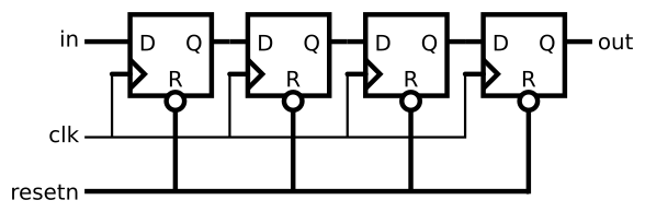
习题:You are given a module my_dff with two inputs and one output (that implements a D flip-flop). Instantiate three of them, then chain them together to make a shift register of length 3. The clk port needs to be connected to all instances.
The module provided to you is: module my_dff ( input clk, input d, output q );
Note that to make the internal connections, you will need to declare some wires. Be careful about naming your wires and module instances: the names must be unique.
习题:You are given a module my_dff8 with two inputs and one output (that implements a set of 8 D flip-flops). Instantiate three of them, then chain them together to make a 8-bit wide shift register of length 3. In addition, create a 4-to-1 multiplexer (not provided) that chooses what to output depending on sel[1:0]: The value at the input d, after the first, after the second, or after the third D flip-flop. (Essentially, sel selects how many cycles to delay the input, from zero to three clock cycles.)
The module provided to you is: module my_dff8 ( input clk, input [7:0] d, output [7:0] q );
The multiplexer is not provided. One possible way to write one is inside an always block with a case statement inside.
习题:You are given a module add16 that performs a 16-bit addition. Instantiate two of them to create a 32-bit adder. One add16 module computes the lower 16 bits of the addition result, while the second add16 module computes the upper 16 bits of the result, after receiving the carry-out from the first adder. Your 32-bit adder does not need to handle carry-in (assume 0) or carry-out (ignored), but the internal modules need to in order to function correctly. (In other words, the add16 module performs 16-bit a + b + cin, while your module performs 32-bit a + b).
Connect the modules together as shown in the diagram below. The provided module add16 has the following declaration: module add16 ( input[15:0] a, input[15:0] b, input cin, output[15:0] sum, output cout );
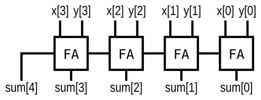
习题:In this exercise, you will create a circuit with two levels of hierarchy. Your top_module will instantiate two copies of add16 (provided), each of which will instantiate 16 copies of add1 (which you must write). Thus, you must write two modules: top_module and add1.
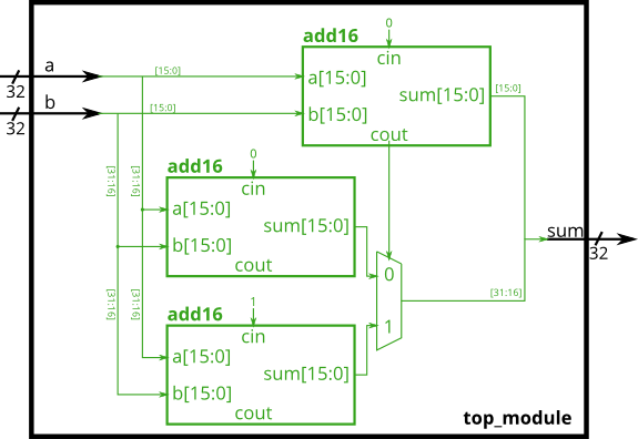
习题:In this exercise, you are provided with the same module add16 as the previous exercise, which adds two 16-bit numbers with carry-in and produces a carry-out and 16-bit sum. You must instantiate three of these to build the carry-select adder, using your own 16-bit 2-to-1 multiplexer.
Connect the modules together as shown in the diagram below. The provided module add16 has the following declaration:
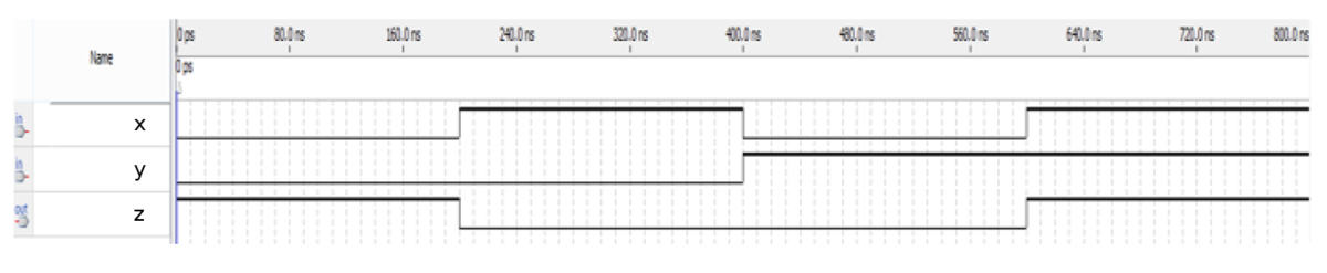
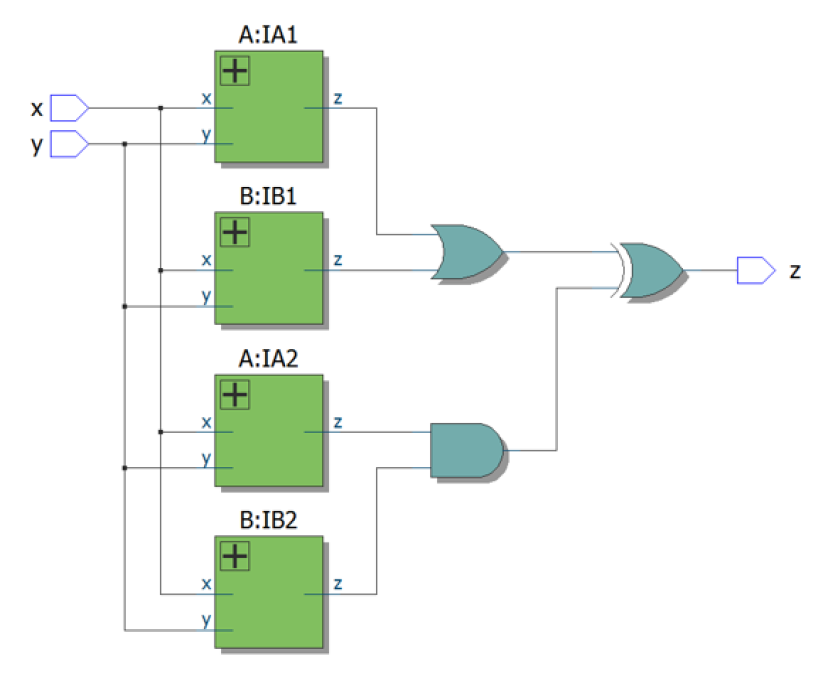
习题:Build an XOR gate three ways, using an assign statement, a combinational always block, and a clocked always block. Note that the clocked always block produces a different circuit from the other two: There is a flip-flop so the output is delayed.
习题:Build a 2-to-1 mux that chooses between a and b. Choose b if both sel_b1 and sel_b2 are true. Otherwise, choose a. Do the same twice, once using assign statements and once using a procedural if statement.
习题:The following code contains incorrect behaviour that creates a latch. Fix the bugs so that you will shut off the computer only if it’s really overheated, and stop driving if you’ve arrived at your destination or you need to refuel.
verilog
always @(*) begin if (cpu_overheated) shut_off_computer = 1;endalways @(*) begin if (~arrived) keep_driving = ~gas_tank_empty;end
习题:Case statements are more convenient than if statements if there are a large number of cases. So, in this exercise, create a 6-to-1 multiplexer. When sel is between 0 and 5, choose the corresponding data input. Otherwise, output 0. The data inputs and outputs are all 4 bits wide.
习题:Build a 4-bit priority encoder. For this problem, if none of the input bits are high (i.e., input is zero), output zero. Note that a 4-bit number has 16 possible combinations.
习题:Build a priority encoder for 8-bit inputs. Given an 8-bit vector, the output should report the first (least significant) bit in the vector that is 1. Report zero if the input vector has no bits that are high.
习题:Suppose you’re building a circuit to process scancodes from a PS/2 keyboard for a game. Given the last two bytes of scancodes received, you need to indicate whether one of the arrow keys on the keyboard have been pressed. This involves a fairly simple mapping, which can be implemented as a case statement (or if-elseif) with four cases.
Scancode [15:0]
Arrow key
16’he06b
left arrow
16’he072
down arrow
16’he074
right arrow
16’he075
up arrow
Anything else
none
Your circuit has one 16-bit input, and four outputs. Build this circuit that recognizes these four scancodes and asserts the correct output.
习题:Given four unsigned numbers, find the minimum. Unsigned numbers can be compared with standard comparison operators (a < b). Use the conditional operator to make two-way min circuits, then compose a few of them to create a 4-way min circuit. You’ll probably want some wire vectors for the intermediate results.
习题:Parity checking is often used as a simple method of detecting errors when transmitting data through an imperfect channel. Create a circuit that will compute a parity bit for a 8-bit byte (which will add a 9th bit to the byte). We will use "even" parity, where the parity bit is just the XOR of all 8 data bits.
习题:Given a 100-bit input vector [99:0], reverse its bit ordering.
给出一个100bit的输入向量,调转每个bit的顺序。
verilog
module top_module ( input [99:0] in, output reg [99:0] out); always @(*)begin int i; for (i = 0; i < 100; i = i + 1) out[i] = in[99-i]; endendmodule
在本题的官方答案中使用了一个函数$bits(),这个函数可以返回一个信号的宽度。
Combinational for-loop: 255-bit population count
习题:A "population count" circuit counts the number of '1’s in an input vector. Build a population count circuit for a 255-bit input vector.
人口计数电路统计一个输入向量中有多少个1。搭建一个255位输入向量的人口计数电路。
verilog
module top_module( input [254:0] in, output [7:0] out ); always @(*)begin int i; out = 1'b0; for (i = 0; i < 255; i = i + 1) if (in[i]) out = out + 1'b1; endendmodule
习题:You are provided with a BCD one-digit adder named bcd_fadd that adds two BCD digits and carry-in, and produces a sum and carry-out.
Instantiate 100 copies of bcd_fadd to create a 100-digit BCD ripple-carry adder. Your adder should add two 100-digit BCD numbers (packed into 400-bit vectors) and a carry-in to produce a 100-digit sum and carry out.
习题:Create a circuit that has two 2-bit inputs A[1:0] and B[1:0], and produces an output z. The value of z should be 1 if A = B, otherwise z should be 0.
搭建一个电路有两个输入和一个输出。当输入相等时输出为1,否则为0。
verilog
module top_module ( input [1:0] A, input [1:0] B, output z ); assign z = (A == B);endmodule
习题:Suppose you are designing a circuit to control a cellphone’s ringer and vibration motor. Whenever the phone needs to ring from an incoming call (input ring), your circuit must either turn on the ringer (output ringer = 1) or the motor (output motor = 1), but not both. If the phone is in vibrate mode (input vibrate_mode = 1), turn on the motor. Otherwise, turn on the ringer.
习题:A heating/cooling thermostat controls both a heater (during winter) and an air conditioner (during summer). Implement a circuit that will turn on and off the heater, air conditioning, and blower fan as appropriate.
The thermostat can be in one of two modes: heating (mode = 1) and cooling (mode = 0). In heating mode, turn the heater on when it is too cold (too_cold = 1) but do not use the air conditioner. In cooling mode, turn the air conditioner on when it is too hot (too_hot = 1), but do not turn on the heater. When the heater or air conditioner are on, also turn on the fan to circulate the air. In addition, the user can also request the fan to turn on (fan_on = 1), even if the heater and air conditioner are off.
Try to use only assign statements, to see whether you can translate a problem description into a collection of logic gates.
习题:A "population count" circuit counts the number of '1’s in an input vector. Build a population count circuit for a 3-bit input vector.
人口计数电路计算一个输入向量中1的个数。搭建一个输入向量是3位的人口计数电路。
verilog
module top_module( input [2:0] in, output [1:0] out ); always @(*) begin int i; out = 0; for (i = 0; i < 3; i = i + 1) begin out = out + in[i]; end endendmodule
习题:You are given a four-bit input vector in[3:0]. We want to know some relationships between each bit and its neighbour:
out_both: Each bit of this output vector should indicate whether both the corresponding input bit and its neighbour to the left (higher index) are '1'. For example, out_both[2] should indicate if in[2] and in[3] are both 1. Since in[3] has no neighbour to the left, the answer is obvious so we don’t need to know out_both[3].
out_any: Each bit of this output vector should indicate whether any of the corresponding input bit and its neighbour to the right are '1'. For example, out_any[2] should indicate if either in[2] or in[1] are 1. Since in[0] has no neighbour to the right, the answer is obvious so we don’t need to know out_any[0].
out_different: Each bit of this output vector should indicate whether the corresponding input bit is different from its neighbour to the left. For example, out_different[2] should indicate if in[2] is different from in[3]. For this part, treat the vector as wrapping around, so in[3]'s neighbour to the left is in[0].
习题:You are given a 100-bit input vector in[99:0]. We want to know some relationships between each bit and its neighbour:
out_both: Each bit of this output vector should indicate whether both the corresponding input bit and its neighbour to the left are '1'. For example, out_both[98] should indicate if in[98] and in[99] are both 1. Since in[99] has no neighbour to the left, the answer is obvious so we don’t need to know out_both[99].
out_any: Each bit of this output vector should indicate whether any of the corresponding input bit and its neighbour to the right are '1'. For example, out_any[2] should indicate if either in[2] or in[1] are 1. Since in[0] has no neighbour to the right, the answer is obvious so we don’t need to know out_any[0].
out_different: Each bit of this output vector should indicate whether the corresponding input bit is different from its neighbour to the left. For example, out_different[98] should indicate if in[98] is different from in[99]. For this part, treat the vector as wrapping around, so in[99]'s neighbour to the left is in[0].
module top_module( input [15:0] a, b, c, d, e, f, g, h, i, input [3:0] sel, output [15:0] out ); always @(*) begin case (sel) 4'd0: out = a; 4'd1: out = b; 4'd2: out = c; 4'd3: out = d; 4'd4: out = e; 4'd5: out = f; 4'd6: out = g; 4'd7: out = h; 4'd8: out = i; default: out = {16{1'b1}}; endcase endendmodule
习题:Create a 1-bit wide, 256-to-1 multiplexer. The 256 inputs are all packed into a single 256-bit input vector. sel=0 should select in[0], sel=1 selects bits in[1], sel=2 selects bits in[2], etc.
习题:Create a 4-bit wide, 256-to-1 multiplexer. The 256 4-bit inputs are all packed into a single 1024-bit input vector. sel=0 should select bits in[3:0], sel=1 selects bits in[7:4], sel=2 selects bits in[11:8], etc.
习题:Assume that you have two 8-bit 2’s complement numbers, a[7:0] and b[7:0]. These numbers are added to produce s[7:0]. Also compute whether a (signed) overflow has occurred.
习题:Create 8 D flip-flops with active high synchronous reset. The flip-flops must be reset to 0x34 rather than zero. All DFFs should be triggered by the negative edge of clk.
习题:Create 16 D flip-flops. It’s sometimes useful to only modify parts of a group of flip-flops. The byte-enable inputs control whether each byte of the 16 registers should be written to on that cycle. byteena[1] controls the upper byte d[15:8], while byteena[0] controls the lower byte d[7:0].
resetn is a synchronous, active-low reset.
All DFFs should be triggered by the positive edge of clk.
Assume that you want to implement hierarchical Verilog code for this circuit, using three instantiations of a submodule that has a flip-flop and multiplexer in it. Write a Verilog module (containing one flip-flop and multiplexer) named top_module for this submodule.
习题:A JK flip-flop has the below truth table.Implement a JK flip-flop with only a D-type flip-flop and gates. Note: Qold is the output of the D flip-flop before the positive clock edge.
习题:For each bit in an 8-bit vector, detect when the input signal changes from 0 in one clock cycle to 1 the next (similar to positive edge detection). The output bit should be set the cycle after a 0 to 1 transition occurs.
习题:For each bit in an 8-bit vector, detect when the input signal changes from one clock cycle to the next (detect any edge). The output bit should be set the cycle after a 0 to 1 transition occurs.
习题:For each bit in a 32-bit vector, capture when the input signal changes from 1 in one clock cycle to 0 the next. "Capture" means that the output will remain 1 until the register is reset (synchronous reset).
Each output bit behaves like a SR flip-flop: The output bit should be set (to 1) the cycle after a 1 to 0 transition occurs. The output bit should be reset (to 0) at the positive clock edge when reset is high. If both of the above events occur at the same time, reset has precedence.
习题:Build a decade counter that counts from 0 through 9, inclusive, with a period of 10. The reset input is synchronous, and should reset the counter to 0. We want to be able to pause the counter rather than always incrementing every clock cycle, so the slowena input indicates when the counter should increment.
习题:From a 1000 Hz clock, derive a 1 Hz signal, called OneHertz, that could be used to drive an Enable signal for a set of hour/minute/second counters to create a digital wall clock. Since we want the clock to count once per second, the OneHertz signal must be asserted for exactly one cycle each second. Build the frequency divider using modulo-10 (BCD) counters and as few other gates as possible. Also output the enable signals from each of the BCD counters you use (c_enable[0] for the fastest counter, c_enable[2] for the slowest).
The following BCD counter is provided for you. Enable must be high for the counter to run. Reset is synchronous and set high to force the counter to zero. All counters in your circuit must directly use the same 1000 Hz signal.
习题:Create a set of counters suitable for use as a 12-hour clock (with am/pm indicator). Your counters are clocked by a fast-running clk, with a pulse on ena whenever your clock should increment (i.e., once per second).
reset resets the clock to 12:00 AM. pm is 0 for AM and 1 for PM. hh, mm, and ss are two BCD (Binary-Coded Decimal) digits each for hours (01-12), minutes (00-59), and seconds (00-59). Reset has higher priority than enable, and can occur even when not enabled.
module top_module( input clk, input reset, input ena, output pm, output [7:0] hh, output [7:0] mm, output [7:0] ss); always @(posedge clk) begin if(reset)begin hh <= 8'h12; mm <= 0; ss <= 0; pm <= 0; end else begin if(ena) begin ss <= ss + 1; if(ss[3:0] == 9) begin ss[3:0] <= 0; ss[7:4] <= ss[7:4] + 1; end if(ss == 8'h59) begin mm <= mm + 1; if(mm[3:0] == 9) begin mm[3:0] <= 0; mm[7:4] <= mm[7:4] + 1; end ss <= 0; end if(ss == 8'h59 & mm == 8'h59) begin hh <= hh + 1; if(hh[3:0] == 9) begin hh[3:0] <= 0; hh[7:4] <= hh[7:4] + 1; end mm <= 0; end if(hh == 8'h11 & ss == 8'h59 & mm == 8'h59) begin pm <= ~pm; end if(hh == 8'h12 & ss == 8'h59 & mm == 8'h59) begin hh <= 8'h01; end end end endendmodule
习题:Build a 100-bit left/right rotator, with synchronous load and left/right enable. A rotator shifts-in the shifted-out bit from the other end of the register, unlike a shifter that discards the shifted-out bit and shifts in a zero. If enabled, a rotator rotates the bits around and does not modify/discard them.
load: Loads shift register with data[99:0] instead of rotating.
ena[1:0]: Chooses whether and which direction to rotate.
习题:Build a 64-bit arithmetic shift register, with synchronous load. The shifter can shift both left and right, and by 1 or 8 bit positions, selected by amount.
An arithmetic right shift shifts in the sign bit of the number in the shift register (q[63] in this case) instead of zero as done by a logical right shift. Another way of thinking about an arithmetic right shift is that it assumes the number being shifted is signed and preserves the sign, so that arithmetic right shift divides a signed number by a power of two.
There is no difference between logical and arithmetic left shifts.
load: Loads shift register with data[63:0] instead of shifting.
ena: Chooses whether to shift.
amount: Chooses which direction and how much to shift.
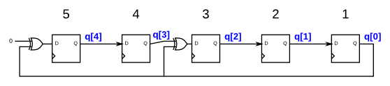
习题:A linear feedback shift register is a shift register usually with a few XOR gates to produce the next state of the shift register. A Galois LFSR is one particular arrangement where bit positions with a "tap" are XORed with the output bit to produce its next value, while bit positions without a tap shift. If the taps positions are carefully chosen, the LFSR can be made to be "maximum-length". A maximum-length LFSR of n bits cycles through 2n−1 states before repeating (the all-zero state is never reached).
The following diagram shows a 5-bit maximal-length Galois LFSR with taps at bit positions 5 and 3. (Tap positions are usually numbered starting from 1). Note that I drew the XOR gate at position 5 for consistency, but one of the XOR gate inputs is 0.
Build this LFSR. The reset should reset the LFSR to 1.
习题:In this question, you will design a circuit for an 8x1 memory, where writing to the memory is accomplished by shifting-in bits, and reading is "random access", as in a typical RAM. You will then use the circuit to realize a 3-input logic function.
First, create an 8-bit shift register with 8 D-type flip-flops. Label the flip-flop outputs from Q[0]…Q[7]. The shift register input should be called S, which feeds the input of Q[0] (MSB is shifted in first). The enable input controls whether to shift. Then, extend the circuit to have 3 additional inputs A,B,C and an output Z. The circuit’s behaviour should be as follows: when ABC is 000, Z=Q[0], when ABC is 001, Z=Q[1], and so on. Your circuit should contain ONLY the 8-bit shift register, and multiplexers. (Aside: this circuit is called a 3-input look-up-table (LUT)).
习题:Rule 90 is a one-dimensional cellular automaton with interesting properties.
The rules are simple. There is a one-dimensional array of cells (on or off). At each time step, the next state of each cell is the XOR of the cell’s two current neighbours. A more verbose way of expressing this rule is the following table, where a cell’s next state is a function of itself and its two neighbours:
Left
Center
Right
Center’s next state
1
1
1
0
1
1
0
1
1
0
1
0
1
0
0
1
0
1
1
1
0
1
0
0
0
0
1
1
0
0
0
0
In this circuit, create a 512-cell system (q[511:0]), and advance by one time step each clock cycle. The load input indicates the state of the system should be loaded with data[511:0]. Assume the boundaries (q[-1] and q[512]) are both zero (off).
习题:Rule 110 is a one-dimensional cellular automaton with interesting properties.
There is a one-dimensional array of cells (on or off). At each time step, the state of each cell changes. In Rule 110, the next state of each cell depends only on itself and its two neighbours, according to the following table:
Left
Center
Right
Center’s next state
1
1
1
0
1
1
0
1
1
0
1
1
1
0
0
0
0
1
1
1
0
1
0
1
0
0
1
1
0
0
0
0
In this circuit, create a 512-cell system (q[511:0]), and advance by one time step each clock cycle. The load input indicates the state of the system should be loaded with data[511:0]. Assume the boundaries (q[-1] and q[512]) are both zero (off).
习题:Conway’s Game of Life is a two-dimensional cellular automaton.
The "game" is played on a two-dimensional grid of cells, where each cell is either 1 (alive) or 0 (dead). At each time step, each cell changes state depending on how many neighbours it has:
0-1 neighbour: Cell becomes 0.
2 neighbours: Cell state does not change.
3 neighbours: Cell becomes 1.
4+ neighbours: Cell becomes 0.
The game is formulated for an infinite grid. In this circuit, we will use a 16x16 grid. To make things more interesting, we will use a 16x16 toroid, where the sides wrap around to the other side of the grid. For example, the corner cell (0,0) has 8 neighbours: (15,1), (15,0), (15,15), (0,1), (0,15), (1,1), (1,0), and (1,15). The 16×16 grid is represented by a length 256 vector, where each row of 16 cells is represented by a sub-vector: q[15:0] is row 0, q[31:16] is row 1, etc. (This tool accepts SystemVerilog, so you may use 2D vectors if you wish.)
load: Loads data into q at the next clock edge, for loading initial state.
q: The 16×16 current state of the game, updated every clock cycle.
The game state should advance by one timestep every clock cycle.
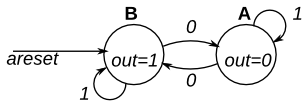
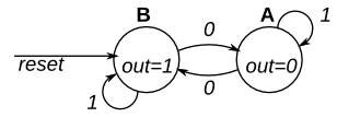
module top_module(clk, reset, in, out); input clk; input reset; input in; output out; reg out; parameter A=0, B=1; reg present_state, next_state; always @(posedge clk) begin if (reset) begin present_state = B; out = B; end else begin case (present_state) A: next_state = in ? A : B; B: next_state = in ? B : A; endcase present_state = next_state; case (present_state) A: out = 0; B: out = 1; endcase end endendmodule
习题:The following is the state transition table for a Moore state machine with one input, one output, and four states. Use the following state encoding: A=2’b00, B=2’b01, C=2’b10, D=2’b11.
Implement only the state transition logic and output logic (the combinational logic portion) for this state machine. Given the current state (state), compute the next_state and output (out) based on the state transition table.
State
Next state (in=0)
Next state (in=1)
Output
A
A
B
0
B
C
B
0
C
A
D
0
D
C
B
1
下面是一个单输入单输出的Moore型状态机的状态转移表。
只实现这个状态机的状态跳转逻辑和输出逻辑。指定当前状态,基于状态转移表计算下一状态和输出。
verilog
module top_module(
    input in,
    input [1:0] state,
    output [1:0] next_state,
    output out); //

    parameter A=0, B=1, C=2, D=3;

    always @(*)begin
        case(state)
            A: next_state = in ? B : A;
            B: next_state = in ? B : C;
            C: next_state = in ? D : A;
            D: next_state = in ? B : C;
        endcase
    end

    assign out = (state == D) ? 1 : 0;

endmodule
习题:The following is the state transition table for a Moore state machine with one input, one output, and four states. Use the following one-hot state encoding: A=4’b0001, B=4’b0010, C=4’b0100, D=4’b1000.
Derive state transition and output logic equations by inspection assuming a one-hot encoding. Implement only the state transition logic and output logic (the combinational logic portion) for this state machine. (The testbench will test with non-one hot inputs to make sure you’re not trying to do something more complicated).
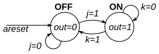
习题:The following is the state transition table for a Moore state machine with one input, one output, and four states. Implement this state machine. Include an asynchronous reset that resets the FSM to state A.
module top_module( input clk, input in, input areset, output out); parameter A=0, B=1, C=2, D=3; reg [1:0] state; reg [1:0] next_state; always @(*) begin case(state) A: next_state = in ? B : A; B: next_state = in ? B : C; C: next_state = in ? D : A; D: next_state = in ? B : C; endcase end always @(posedge clk or posedge areset) begin if(areset)state <= A; else state <= next_state; end assign out = (state == D);endmodule
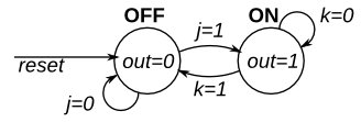
习题:The following is the state transition table for a Moore state machine with one input, one output, and four states. Implement this state machine. Include a synchronous reset that resets the FSM to state A.
习题:A large reservoir of water serves several users. In order to keep the level of water sufficiently high, three sensors are placed vertically at 5-inch intervals. When the water level is above the highest sensor (S3), the input flow rate should be zero. When the level is below the lowest sensor (S1), the flow rate should be at maximum (both Nominal flow valve and Supplemental flow valve opened). The flow rate when the level is between the upper and lower sensors is determined by two factors: the water level and the level previous to the last sensor change. Each water level has a nominal flow rate associated with it, as shown in the table below. If the sensor change indicates that the previous level was lower than the current level, the nominal flow rate should take place. If the previous level was higher than the current level, the flow rate should be increased by opening the Supplemental flow valve (controlled by ΔFR). Draw the Moore model state diagram for the water reservoir controller. Clearly indicate all state transitions and outputs for each state. The inputs to your FSM are S1, S2 and S3; the outputs are FR1, FR2, FR3 and ΔFR.
Also include an active-high synchronous reset that resets the state machine to a state equivalent to if the water level had been low for a long time (no sensors asserted, and all four outputs asserted).
习题:The game Lemmings involves critters with fairly simple brains. So simple that we are going to model it using a finite state machine.
In the Lemmings’ 2D world, Lemmings can be in one of two states: walking left or walking right. It will switch directions if it hits an obstacle. In particular, if a Lemming is bumped on the left, it will walk right. If it’s bumped on the right, it will walk left. If it’s bumped on both sides at the same time, it will still switch directions.
Implement a Moore state machine with two states, two inputs, and one output that models this behaviour.
习题:In addition to walking left and right, Lemmings will fall (and presumably go "aaah!") if the ground disappears underneath them.
In addition to walking left and right and changing direction when bumped, when ground=0, the Lemming will fall and say "aaah!". When the ground reappears (ground=1), the Lemming will resume walking in the same direction as before the fall. Being bumped while falling does not affect the walking direction, and being bumped in the same cycle as ground disappears (but not yet falling), or when the ground reappears while still falling, also does not affect the walking direction.
Build a finite state machine that models this behaviour.
习题:In addition to walking and falling, Lemmings can sometimes be told to do useful things, like dig (it starts digging when dig=1). A Lemming can dig if it is currently walking on ground (ground=1 and not falling), and will continue digging until it reaches the other side (ground=0). At that point, since there is no ground, it will fall (aaah!), then continue walking in its original direction once it hits ground again. As with falling, being bumped while digging has no effect, and being told to dig when falling or when there is no ground is ignored.
(In other words, a walking Lemming can fall, dig, or switch directions. If more than one of these conditions are satisfied, fall has higher precedence than dig, which has higher precedence than switching directions.)
Extend your finite state machine to model this behaviour.
习题:Although Lemmings can walk, fall, and dig, Lemmings aren’t invulnerable. If a Lemming falls for too long then hits the ground, it can splatter. In particular, if a Lemming falls for more than 20 clock cycles then hits the ground, it will splatter and cease walking, falling, or digging (all 4 outputs become 0), forever (Or until the FSM gets reset). There is no upper limit on how far a Lemming can fall before hitting the ground. Lemmings only splatter when hitting the ground; they do not splatter in mid-air.
Extend your finite state machine to model this behaviour.
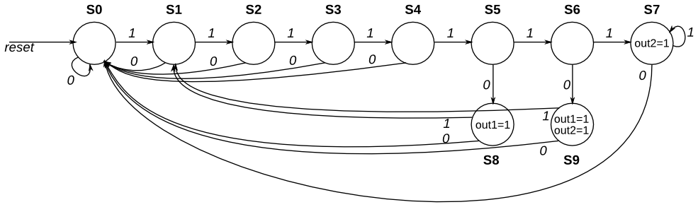
习题:Given the following state machine with 1 input and 2 outputs:
Suppose this state machine uses one-hot encoding, where state[0] through state[9] correspond to the states S0 though S9, respectively. The outputs are zero unless otherwise specified.
Implement the state transition logic and output logic portions of the state machine (but not the state flip-flops). You are given the current state in state[9:0] and must produce next_state[9:0] and the two outputs. Derive the logic equations by inspection assuming a one-hot encoding. (The testbench will test with non-one hot inputs to make sure you’re not trying to do something more complicated).
习题:The PS/2 mouse protocol sends messages that are three bytes long. However, within a continuous byte stream, it’s not obvious where messages start and end. The only indication is that the first byte of each three byte message always has bit[3]=1 (but bit[3] of the other two bytes may be 1 or 0 depending on data).
We want a finite state machine that will search for message boundaries when given an input byte stream. The algorithm we’ll use is to discard bytes until we see one with bit[3]=1. We then assume that this is byte 1 of a message, and signal the receipt of a message once all 3 bytes have been received (done).
The FSM should signal done in the cycle immediately after the third byte of each message was successfully received.
习题:Now that you have a state machine that will identify three-byte messages in a PS/2 byte stream, add a datapath that will also output the 24-bit (3 byte) message whenever a packet is received (out_bytes[23:16] is the first byte, out_bytes[15:8] is the second byte, etc.).
out_bytes needs to be valid whenever the done signal is asserted. You may output anything at other times (i.e., don’t-care).
习题:In many (older) serial communications protocols, each data byte is sent along with a start bit and a stop bit, to help the receiver delimit bytes from the stream of bits. One common scheme is to use one start bit (0), 8 data bits, and 1 stop bit (1). The line is also at logic 1 when nothing is being transmitted (idle).
Design a finite state machine that will identify when bytes have been correctly received when given a stream of bits. It needs to identify the start bit, wait for all 8 data bits, then verify that the stop bit was correct. If the stop bit does not appear when expected, the FSM must wait until it finds a stop bit before attempting to receive the next byte.
习题:Now that you have a finite state machine that can identify when bytes are correctly received in a serial bitstream, add a datapath that will output the correctly-received data byte. out_byte needs to be valid when done is 1, and is don’t-care otherwise.
Note that the serial protocol sends the least significant bit first.
习题:We want to add parity checking to the serial receiver. Parity checking adds one extra bit after each data byte. We will use odd parity, where the number of 1s in the 9 bits received must be odd. For example, 101001011 satisfies odd parity (there are 5 1s), but 001001011 does not.
Change your FSM and datapath to perform odd parity checking. Assert the done signal only if a byte is correctly received and its parity check passes. Like the serial receiver FSM, this FSM needs to identify the start bit, wait for all 9 (data and parity) bits, then verify that the stop bit was correct. If the stop bit does not appear when expected, the FSM must wait until it finds a stop bit before attempting to receive the next byte.
You are provided with the following module that can be used to calculate the parity of the input stream (It’s a TFF with reset). The intended use is that it should be given the input bit stream, and reset at appropriate times so it counts the number of 1 bits in each byte.
verilog
module parity ( input clk, input reset, input in, output reg odd); always @(posedge clk) if (reset) odd <= 0; else if (in) odd <= ~odd;endmodule
习题:Synchronous HDLC framing involves decoding a continuous bit stream of data to look for bit patterns that indicate the beginning and end of frames (packets). Seeing exactly 6 consecutive 1s (i.e., 01111110) is a "flag" that indicate frame boundaries. To avoid the data stream from accidentally containing "flags", the sender inserts a zero after every 5 consecutive 1s which the receiver must detect and discard. We also need to signal an error if there are 7 or more consecutive 1s.
Create a finite state machine to recognize these three sequences:
0111110: Signal a bit needs to be discarded (disc).
01111110: Flag the beginning/end of a frame (flag).
01111111…: Error (7 or more 1s) (err).
When the FSM is reset, it should be in a state that behaves as though the previous input were 0.
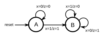
习题:Implement a Mealy-type finite state machine that recognizes the sequence "101" on an input signal named x. Your FSM should have an output signal, z, that is asserted to logic-1 when the "101" sequence is detected. Your FSM should also have an active-low asynchronous reset. You may only have 3 states in your state machine. Your FSM should recognize overlapping sequences.
习题:You are to design a one-input one-output serial 2’s complementer Moore state machine. The input (x) is a series of bits (one per clock cycle) beginning with the least-significant bit of the number, and the output (Z) is the 2’s complement of the input. The machine will accept input numbers of arbitrary length. The circuit requires an asynchronous reset. The conversion begins when Reset is released and stops when Reset is asserted.
习题:Consider a finite state machine with inputs s and w. Assume that the FSM begins in a reset state called A, as depicted below. The FSM remains in state A as long as s = 0, and it moves to state B when s = 1. Once in state B the FSM examines the value of the input w in the next three clock cycles. If w = 1 in exactly two of these clock cycles, then the FSM has to set an output z to 1 in the following clock cycle. Otherwise z has to be 0. The FSM continues checking w for the next three clock cycles, and so on. The timing diagram below illustrates the required values of z for different values of w.
Use as few states as possible. Note that the s input is used only in state A, so you need to consider just the w input.
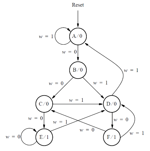
习题:Consider the state machine shown below, which has one input w and one output z.
Assume that you wish to implement the FSM using three flip-flops and state codes y[3:1] = 000, 001, … , 101 for states A, B, … , F, respectively. Show a state-assigned table for this FSM. Derive a next-state expression for the flip-flop y[2].
Implement just the next-state logic for y[2]. (This is much more a FSM question than a Verilog coding question. Oh well.)
module top_module ( input [3:1] y, input w, output Y2); reg [3:1] Y; always @(*)begin case(y) 3'b000: Y = w ? 3'b000 : 3'b001; 3'b001: Y = w ? 3'b011 : 3'b010; 3'b010: Y = w ? 3'b011 : 3'b100; 3'b011: Y = w ? 3'b000 : 3'b101; 3'b100: Y = w ? 3'b011 : 3'b100; 3'b101: Y = w ? 3'b011 : 3'b010; endcase end assign Y2 = Y[2];endmodule
习题:Consider the state machine shown below, which has one input w and one output z.
For this part, assume that a one-hot code is used with the state assignment y[6:1] = 000001, 000010, 000100, 001000, 010000, 100000 for states A, B,…, F, respectively.
Write a logic expression for the next-state signals Y2 and Y4. (Derive the logic equations by inspection assuming a one-hot encoding. The testbench will test with non-one hot inputs to make sure you’re not trying to do something more complicated).
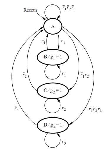
习题:Consider the FSM described by the state diagram shown below:
This FSM acts as an arbiter circuit, which controls access to some type of resource by three requesting devices. Each device makes its request for the resource by setting a signal r[i] = 1, where r[i] is either r[1], r[2], or r[3]. Each r[i] is an input signal to the FSM, and represents one of the three devices. The FSM stays in state A as long as there are no requests. When one or more request occurs, then the FSM decides which device receives a grant to use the resource and changes to a state that sets that device’s g[i] signal to 1. Each g[i] is an output from the FSM. There is a priority system, in that device 1 has a higher priority than device 2, and device 3 has the lowest priority. Hence, for example, device 3 will only receive a grant if it is the only device making a request when the FSM is in state A. Once a device, i, is given a grant by the FSM, that device continues to receive the grant as long as its request, r[i] = 1.
Write complete Verilog code that represents this FSM. Use separate always blocks for the state table and the state flip-flops, as done in lectures. Describe the FSM outputs, g[i], using either continuous assignment statement(s) or an always block (at your discretion). Assign any state codes that you wish to use.
习题:Consider a finite state machine that is used to control some type of motor. The FSM has inputs x and y, which come from the motor, and produces outputs f and g, which control the motor. There is also a clock input called clk and a reset input called resetn.
The FSM has to work as follows. As long as the reset input is asserted, the FSM stays in a beginning state, called state A. When the reset signal is de-asserted, then after the next clock edge the FSM has to set the output f to 1 for one clock cycle. Then, the FSM has to monitor the x input. When x has produced the values 1, 0, 1 in three successive clock cycles, then g should be set to 1 on the following clock cycle. While maintaining g = 1 the FSM has to monitor the y input. If y has the value 1 within at most two clock cycles, then the FSM should maintain g = 1 permanently (that is, until reset). But if y does not become 1 within two clock cycles, then the FSM should set g = 0 permanently (until reset).